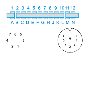
1. Luminanza (S-video Y)
2. GND
3. Audio out
4. Composite video
5. Audio in (max 3 Volt)
6. Chroma (S-video C)
7. N.C.
8. +5V (N.C. nelle prime versioni)
1. GND
2. GND
3. Rosso (RGB)
4. Verde (RGB)
5. Blu (RGB)
6. Intensità
7. Monocromatico
8. Sync orizzontale
9. Sync verticale
1. _SRQ
2. GND
3. ATN (Attention)
4. Clock
5. Data
6. _Reset
1 | GND | |
2 | +5V | +5V (100 mA max) |
3 | /RESET | Reset, usato anche per resettare il device collegato |
4 | CNT1 | Countatore1, CIA #1 |
5 | SP1 | Porta seriale 1, CIA #1 |
6 | CNT2 | Contatore 2, CIA #2 |
7 | SP2 | Porta seriale 2, CIA #2 |
8 | /PC2 | Handshaking, CIA #2 |
9 | ATN | Serial attention in |
10 | 9VAC | 9 VAC (100 mA max) |
11 | 9VAC | 9 VAC (100 mA max) |
12 | GND |
A | GND | |
B | /FLAG2 | Flag 2 |
C | PB0 | Data 0 |
D | PB1 | Data 1 |
E | PB2 | Data 2 |
F | PB3 | Data 3 |
H | PB4 | Data 4 |
J | PB5 | Data 5 |
K | PB6 | Data 6 |
L | PB7 | Data 7 |
M | PA2 | PA2 |
N | GND |
1 | GND | |
2 | +5V | +5V (100 mA max) |
3 | /RESET | Reset, usato anche per resettare il device collegato |
4 | P2 | Data 2 |
5 | P3 | Data 3 |
6 | P4 | Data 4 |
7 | P5 | Data 5 |
8 | RCLK | Ricezione Clock |
9 | ATN | Serial attention in |
10 | 9VAC | 9 VAC (100 mA max) |
11 | 9VAC | 9 VAC (100 mA max) |
12 | GND |
A | GND | |
B | P0 | Data 0 |
C | RXD | RX data |
D | Rt0 | Request t0 send |
E | DTR | Data Terminal Ready |
F | P7 | Data 7 |
H | DCD | Data Carrier Detect |
J | P6 | Data 6 |
K | P1 | Data 1 |
L | DSR | DataSet pronto |
M | TXD | TX data |
N | GND |
1 | GND | |
2 | VIDEO | |
3 | /SRQ IN | |
4 | /EOI | Data 2 |
5 | DIAG | Data 3 |
6 | #2 CAS RD | Lettura cassette #2 |
7 | CAS WR | Scrittura cassette |
8 | #1 CAS RD | Lettura cassette #1 |
9 | VDRIVE | Drive verticale |
10 | HDRIVE | Drive orizzontale |
11 | GRAPHIC | 9 VAC (100 mA max) |
12 | GND |
A | GND | |
B | CA1 | |
C | PA0 | Data 0 |
D | PA1 | Data 1 |
E | PA2 | Data 2 |
F | PA3 | Data 3 |
H | PA4 | Data 4 |
J | PA5 | Data 5 |
K | PA6 | Data 6 |
L | V7 | |
M | CB2 | |
N | GND |
1. GND / N.C.
2. GND (nero)
3. GND / N.C.
4. N.C. (Su VIC20: +5V o N.C.)
5. +5V (rosso)
6. 9V ~ (marrone)
7. 9V ~ (bianco)
1. +5V (rosso)
2. GND (nero)
3. 9V ~ (marrone)
4. 9V ~ (bianco)
1. +5V (1A)
2. GND
3. 9V ~ (0,75A)
4. 9V ~
Interno: GND
Esterno: +9V (0,8A)
PIN | PORTA 1 | PORTA 2 (no VIC20) |
DESCRIZIONE |
---|---|---|---|
1 | JOY A0 | JOY B0 | SU |
2 | JOY A1 | JOY B1 | GIU |
3 | JOY A2 | JOY B2 | SINISTRA |
4 | JOY A3 | JOY B3 | DESTRA |
5 | POT AY | POT BY | INGRESSO Y |
6 | PULS. A | PULS. B | FUOCO |
7 | +5 VOLT | +5 VOLT | 100mA MAX |
8 | GND | GND | |
9 | POT AX | POT BX | INGRESSO X |
PIN | PORTA 1 | PORTA 2 | DESCRIZIONE |
---|---|---|---|
1 | JOY A0 | JOY B0 | SU |
2 | JOY A1 | JOY B1 | GIU |
3 | JOY A2 | JOY B2 | SINISTRA |
4 | JOY A3 | JOY B3 | DESTRA |
5 | +5V DC | +5V DC | |
6 | PULS. A | PULS. B | FUOCO |
7 | GND | GND | |
8 | DATA 2 | DATA 1 | SELECT |
Pin | Segnale | Direzione (da C64) | Significato |
---|---|---|---|
1 | GND | PWR | Ground |
2-3 | +5V DC | PWR | +5V DC |
4 | _IRQ | In | Interrupt Request |
5 | R/_W | Out | Read or _Write indicator |
6 | DOT Clk | Out | Dot clock frequency |
7 | _IO1 | Out | Input/Output area 1 indicator |
8 | _GAME | In | Game configuration |
9 | _EXROM | In | External ROM |
10 | _IO2 | Out | Input/Output area 2 indicator |
11 | _ROML | Out | ROM Low |
12 | BA | Out | Bus Available |
13 | _DMA | In | Direct Memory Access |
14 | D7 | IO | Data line 7 |
15 | D6 | IO | Data line 6 |
16 | D5 | IO | Data line 5 |
17 | D4 | IO | Data line 4 |
18 | D3 | IO | Data line 3 |
19 | D2 | IO | Data line 2 |
20 | D1 | IO | Data line 1 |
21 | D0 | IO | Data line 0 |
22-A | GND | PWR | Ground |
B | _ROMH | Out | ROM High |
C | _RESET | In | Reset |
D | _NMI | In | Non Maskable Interrupt |
E | PHI2 | Out | Phase 2 clock |
F | A15 | Out | Address line 15 |
H | A14 | Out | Address line 14 |
J | A13 | Out | Address line 13 |
K | A12 | Out | Address line 12 |
L | A11 | Out | Address line 11 |
M | A10 | Out | Address line 10 |
N | A9 | Out | Address line 9 |
P | A8 | Out | Address line 8 |
R | A7 | Out | Address line 7 |
S | A6 | Out | Address line 6 |
T | A5 | Out | Address line 5 |
U | A4 | Out | Address line 4 |
V | A3 | Out | Address line 3 |
W | A2 | Out | Address line 2 |
X | A1 | Out | Address line 1 |
Y | A0 | Out | Address line 0 |
Z | GND | PWR | Ground |
Pin | Signal | Description | Comment |
---|---|---|---|
1 | GND | Ground | (0 Volt) |
2 | D0 | data line 0 | data bus of the computer |
3 | D1 | data line 1 | |
4 | D2 | data line 2 | |
5 | D3 | data line 3 | |
6 | D4 | data line 4 | |
7 | D5 | data line 5 | |
8 | D6 | data line 6 | |
9 | D7 | data line 7 | |
10 | /BLK 1 | Memory block 1 | Chip select for block 1; active-low, if address on bus is within $2000-$3FFF. |
11 | /BLK 2 | Memory block 2 | Chip select for block 2; active-low, if address on bus is within $4000-$5FFF. |
12 | /BLK 3 | Memory block 3 | Chip select for block 3; active-low, if address on bus is within $6000-$7FFF. |
13 | /BLK 5 | Memory block 5 | Chip select for block 5; active-low, if address on bus is within $A000-$BFFF. |
14 | /RAM 1 | RAM 1 | Chip select for RAM (memory area $0400 – $07FF) |
15 | /RAM 2 | RAM 2 | Chip select for RAM (memory area $0800 – $0BFF) |
16 | /RAM 3 | RAM 3 | Chip select for RAM (memory area $0C00 – $0FFF) |
17 | V R/W | VIC Read – /Write | high during read cycle, low during write cycle of the VIC |
18 | C R/W | CPU Read – /Write | high during read cycle, low during write cycle of the CPU |
19 | /IRQ | Interrupt Request | Interrupt Request Line |
20 | NC | not connected | |
21 | +5V DC | Supply Voltage +5V DC | + 5 Volt DC. |
22 | GND | Ground | (0 Volt) |
A | GND | Ground | (0 Volt) |
B | A0 | address line 0 | adress bus of the computer |
C | A1 | address line 1 | |
D | A2 | address line 2 | |
E | A3 | address line 3 | |
F | A4 | address line 4 | |
H | A5 | address line 5 | |
J | A6 | address line 6 | |
K | A7 | address line 7 | |
L | A8 | address line 8 | |
M | A9 | address line 9 | |
N | A10 | address line 10 | |
P | A11 | address line 11 | |
R | A12 | address line 12 | |
S | A13 | address line 13 | |
T | /I/O2 | input/output 2 | input/output area 2 ; active low, if address on the bus is within $9800-$9BFF. |
U | /I/O3 | input/output 3 | input/output area 3 ; active low, if address on the bus is within $9C00-$9FFF. |
V | SØ2 | S Phi 2 | system clock (1,108MHz for PAL, 1,018MHz for NTSC) |
W | /NMI | non maskable interrupt | Non Maskable Interrupt Line |
X | /RESET | Reset | If you pull this line to low, all chips will be re-initialized. The program counter of the CPU will be loaded with the reset-vector $FFFC and $FFFD (usually $FD22). |
Y | NC | not connected | |
Z | GND | Ground | (0 Volt) |
PIN | SEGNALE | PIN | SEGNALE |
---|---|---|---|
1 | GND | A | GND |
2 | +5V DC | B | C1 Low |
3 | +5V DC | C | _Reset |
4 | _IRQ | D | RAS |
5 | R/_W | E | Ø0 |
6 | C1 High | F | A15 |
7 | C2 Low | H | A14 |
8 | C2 High | J | A13 |
9 | _CS1 ($C000-$FFFF) | K | A12 |
10 | _CS0 ($8000-$BFFF) | L | A11 |
11 | CAS | M | A10 |
12 | Mux | N | A9 |
13 | BA | P | A8 |
14 | D7 | R | A7 |
15 | D6 | S | A6 |
16 | D5 | T | A5 |
17 | D4 | U | A4 |
18 | D3 | V | A3 |
19 | D2 | W | A2 |
20 | D1 | X | A1 |
21 | D0 | Y | A0 |
22 | AEC | Z | N.C. |
23 | Audio in | AA | N.C. |
24 | Ø2 | BB | N.C. |
25 | GND | CC | GND |
Biscotto | Durata | Descrizione |
---|---|---|
cookielawinfo-checkbox-analytics | 11 months | This cookie is set by GDPR Cookie Consent plugin. The cookie is used to store the user consent for the cookies in the category "Analytics". |
cookielawinfo-checkbox-functional | 11 months | The cookie is set by GDPR cookie consent to record the user consent for the cookies in the category "Functional". |
cookielawinfo-checkbox-necessary | 11 months | This cookie is set by GDPR Cookie Consent plugin. The cookies is used to store the user consent for the cookies in the category "Necessary". |
cookielawinfo-checkbox-others | 11 months | This cookie is set by GDPR Cookie Consent plugin. The cookie is used to store the user consent for the cookies in the category "Other. |
cookielawinfo-checkbox-performance | 11 months | This cookie is set by GDPR Cookie Consent plugin. The cookie is used to store the user consent for the cookies in the category "Performance". |
viewed_cookie_policy | 11 months | The cookie is set by the GDPR Cookie Consent plugin and is used to store whether or not user has consented to the use of cookies. It does not store any personal data. |